Kepler Computing Emerges with $468M to Tackle AI Memory
Stealth chip startup Kepler Computing has unveiled a new high-bandwidth memory architecture, claiming it can bypass expensive lithography and ease the
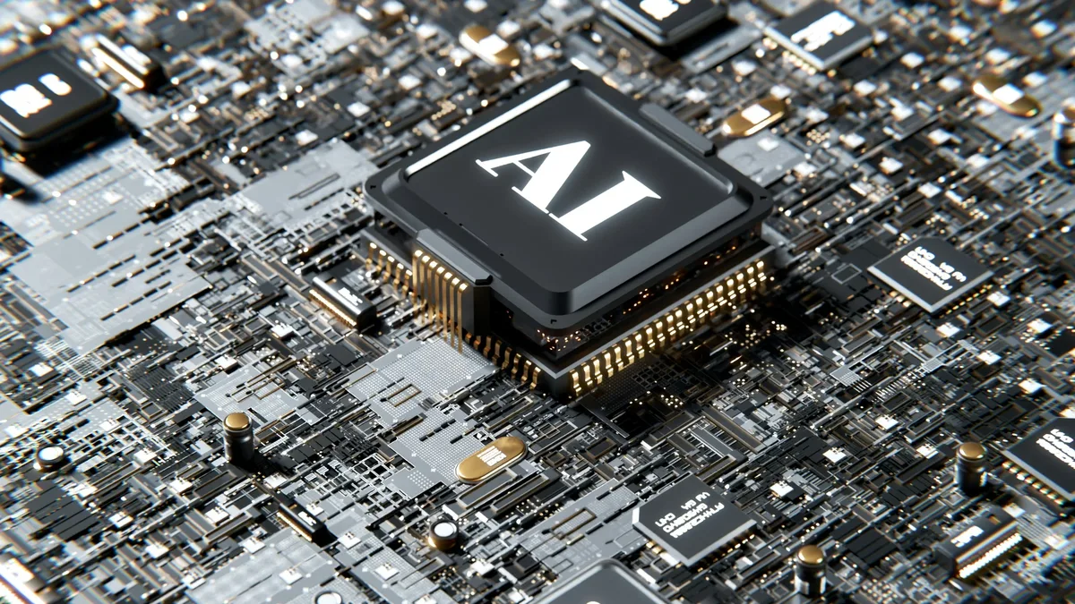
Kepler Computing, a San Jose-based startup founded in 2018, has emerged from stealth with $468 million in funding and a new approach to building memory chips. The company claims its 3D stacking and novel ferroelectric materials can increase memory density without relying on extreme ultraviolet lithography (EUV), addressing a critical bottleneck for AI computing.
The Kepler Approach
While traditional chipmakers use EUV to shrink transistors, Kepler says its method sidesteps this expensive process entirely. The startup's pitch is twofold: it has developed a novel 3D-manufacturing technique for high-bandwidth memory (HBM) and uses a new composite ferroelectric material to improve the density of SRAM cache memory.
Sasi Manipatruni, Kepler's chief technology officer, says the team tested 35 iterations of composites before finding a suitable material class. "Once we found a way to solve the physics problem-as in the physical limitations for HBM-we came up with a material innovation that helps with the amount of memory you can have between chips," he told Wired.
Funding and Fabrication Partners
The company's substantial funding comes from notable backers including Intel Capital, AMD Ventures, Baillie Gifford, and Bill Gates through his Gates Frontier fund. A key manufacturing partner and investor is GlobalFoundries, which committed $50 million. In July, the US Department of Commerce pledged up to $245 million to support Kepler's development of a new class of AI memory technology in the United States.
Current testing and production occur in "mini fabs" in Singapore, use GlobalFoundries' 28-nanometer facilities. Kepler claims it converted a fab into a "next-generation" operation in eight months, compared to a typical 24-month timeframe.
Ed Kaste, senior vice president of GlobalFoundries' CMOS business, endorsed the strategy. "Kepler’s approach is at the sweet spot of our strategy," Kaste said. "It’s a new materials system, with multigenerational scaling potential, without having to build entirely new systems in the fab or invest in very expensive lithography equipment."
Market Timing and Production Roadmap
Kepler's leadership says the AI boom created urgent demand for their HBM alternative. "With the launch of ChatGPT [in 2022] and the explosion of demand for an HBM alternative, we started working on our HBM road map." said CEO Debo Olaosebikan.
The company's production plans are outlined below.
To date, Kepler has run its technology on approximately 2,000 wafers.
Scaling Challenges
Scaling the technology presents significant hurdles, particularly concerning material contamination. Kaste noted that Kepler's composite includes iron, which is "a tough contaminant to introduce into a production facility." He stated the solution must run on dedicated equipment or be fully encapsulated.
Olaosebikan was cryptic about the composite's specifics. "What I can say is, we’re using a small number of materials, and some of them aren’t what you’d typically find in mainstream ferroelectrics," he said.
Industry analysts note the universal difficulty of scaling semiconductor innovations. "The question is how to overcome all the limitations of contamination, different materials, and different tooling, in such a way that the resulting innovation can be used at scale and is worth the cost," said chip analyst Austin Lyons of Creative Strategies. Kepler is betting its retooling costs will be far lower than the $20 billion to $40 billion required to build new fabs.